RecursosElectron tubes, crystals, delay lines (IEC 60617)
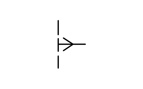
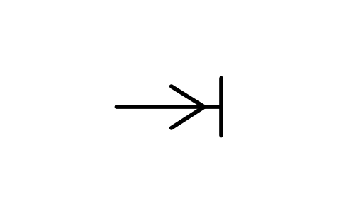
Junction on layer, P region symbol (DWG block)
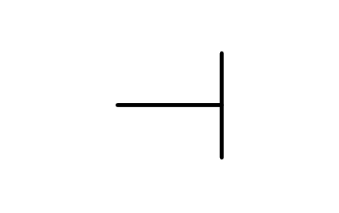
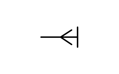
Junction on layer, P region is a ready-to-use AutoCAD block named SEM_S00620_JUNCTION_ON_LAYER_P_REGION in the Electron tubes, crystals, delay lines (IEC 60617), group “Semiconductor regions and channels”. It carries 4 attributes, 0 of them visible, so it works in equipment lists and BlockSync exports.
Block details
| Block name | SEM_S00620_JUNCTION_ON_LAYER_P_REGION |
|---|---|
| Library | Electron tubes, crystals, delay lines (IEC 60617) |
| Group | Semiconductor regions and channels |
| Standard | IEC 60617-5 |
| Attributes | 4 attributes, 0 visible |
Attributes
Hidden, they carry the data for schedules: REMARKS, STD_CLAUSE, STD_REF, DESC.
Export the attributes of every copy in a drawing to Excel with BlockSync, check them and write the corrections back in one run.
How to use it
- Download the ZIP and unzip it. It holds one DWG with the block SEM_S00620_JUNCTION_ON_LAYER_P_REGION.
- Open the DWG and copy the block into your drawing, or insert it from the DWG with INSERT.
- Double-click a copy to fill in the tag and the other attributes.
The symbol is our own drawing after the common form of IEC 60617-5, not a certified copy. The library page explains how the symbols relate to the standard.
Names in other languages
The same symbol under its name in the other site languages.
- inglês
- Junction on layer, P region
- chinês simplificado
- 层上结,P 区
- chinês tradicional
- 層上結,P 區
- japonês
- 層上の接合(P領域)
- coreano
- 층 위 접합, P 영역
- alemão
- Übergang auf Schicht, P-Zone
- francês
- Jonction sur couche, zone P
- italiano
- Giunzione su strato, regione P
- espanhol
- Unión sobre capa, región P